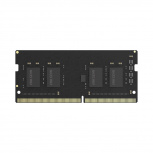
Otros productos similares

A un vistazo
16 internal banks
Bank Grouping is applied, and CAS to CAS latency (tCCD_L, tCCD_S) for the banks in the same or different bank group accesses are available
Bi-Directional Differential Data Strobe
8 bit pre-fetch
Burst Length (BL) switch on-the-fly BL8 or BC4(Burst Chop)
Supports ECC error correction and detection
On-Die Termination (ODT)
Temperature sensor with integrated SPD
This product is in compliance with the RoHS directive
Per DRAM Addressability is supported
Internal Vref DQ level generation is available
Write CRC is supported at all speed grades
CA parity (Command/Address Parity) mode is supported
Detalles del producto
Preguntas y respuestas sobre este producto
Aún no hay preguntas acerca de este producto
Resuelve tus dudas preguntando a la comunidad y a nuestro equipo de servicio al cliente.
Resuelve tus dudas preguntando a la comunidad y a nuestro equipo de servicio al cliente.
Frecuentemente se compran juntos


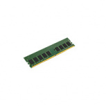
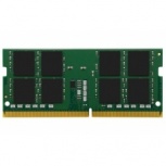
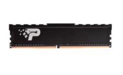
Especificaciones
| Peso y dimensiones | |
|---|---|
| Altura | 31.2 mm |
| Ancho | 133.3 mm |
| Detalles técnicos | |
|---|---|
| Sustainability certificates | RoHS |
| Memoria | |
|---|---|
| Latencia CAS | CL19 |
| Diseño de memoria (módulos x tamaño) | 1 x 16GB |
| Componente para | PC/servidor |
| Voltaje de memoria | 1.2 V |
| Configuración de módulos | 2048M x 72 |
| Tiempo activo en fila | 32 ns |
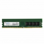
| Tipo de memoria interna | DDR4 |
| Capacidad de memoria RAM | 16GB |
| Velocidad de memoria del reloj | 2666MHz |
| ECC |

|
| Tiempo de ciclo de fila | 46.25 ns |
| Tiempo de actualización de ciclo de fila | 350 ns |
| Otras características | |
|---|---|
| Factor de forma | 288-pin DIMM |
| Condiciones ambientales | |
|---|---|
| Intervalo de temperatura operativa | 0 - 85 °C |
| Intervalo de temperatura de almacenaje | -55 - 100 °C |
Mostrar más
¿Ves alguna información equivocada? Repórtala aquí
Acerca del Fabricante
Otros productos que podrían interesarte
-
 Firewall Cisco Meraki MX95, Alámbrico, 2000...$109,999.00
 -

-
-


Regresar arriba ▲


 100% Productos nuevos